|
Excellent Integrated System LIMITED
|
Gold Index: 17691
You are here: home > Integrated Circuit > DS90C124QVS
.gif)
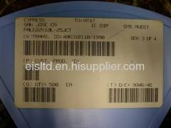
DS90C124QVS
| Price: | 4.3~5.5 USD |
| Payment Terms: | T/T,L/C,WU;PAYPAL |
| Place of Origin: | USA |
|
|
|
| Add to My Favorites | |
| HiSupplier Escrow |
Product Detail
Model No.:
DS90C124QVS
Production Capacity:
10000pcs/month
Delivery Date:
IN STOCK
Type:
Others
Supply Voltage:
Email us
Operating Temperature:
Email us
Means of Transport:
Air
Packing:
TQFP-48
Application:
Others
Brand Name:
National Semiconductor [NS]
Dissipation Power:
john(at)eis-ic.com
john(at)eis-ic.com:
john(at)eis-ic.com
5MHz to 35MHz, DC-Balanced 24-Bit LVDS Deserializer, 48-pin TQFP package
Company Name: Excellent Integrated System LIMITED
Contact Person : John
Email/Msn :John(at)eis-ic.com
Tel : 00852-30777742
Add.: RM 906, WORKINGBERG COMM BLDG, 41-47 MARBLE RD, HONGKONG
Excellent Integrated System LIMITED (EIS LIMITED), Established in 1991, is a professional independent stocking distributor of electronic components and specialize in buying the EXCESS STOCK from the original equipment manufacturers (OEMs), Contract equipment manufacturers (CEMs), and many other factories. EIS has gained good experiences in Excess Inventory Management through its development over 20 years and has become the reliable partner for the domestic and foreign OEM manufacturers. If any inquiry and question,please email us: john(at)eis-ic.com.
PART NUMBER | DS90C124QVS |
BRAND | National Semiconductor [NS] |
PACKAGING | TQFP-48 |
DATE CODE | 12+ |
PRICE | 4.35~5.5USD |
Summary | 5MHz to 35MHz, DC-Balanced 24-Bit LVDS Deserializer, 48-pin TQFP package |
Description as follow:
The DS90C124QVS is a DC-Balanced 24-Bit LVDS Deserializer. The DS90C124QVS incorporates LVDS signaling on the high-speed I/O. LVDS provides a low power and low noise environment for reliably transferring data over a serial transmission path. In addition the DS90C124QVS features pre-emphasis to boost signals over longer distances using lossy cables. Internal DC balanced encoding/decoding is used to support AC-Coupled interconnects.
Parametrics
DS90C124QVS absolute maximum ratings: (1)Supply Voltage (VCC):-0.3V to +4V; (2)LVCMOS/LVTTL Input Voltage:-0.3V to (VCC +0.3V); (3)LVCMOS/LVTTL Output Voltage:-0.3V to (VCC +0.3V); (4)LVDS Receiver Input Voltage:-0.3V to 3.9V; (5)LVDS Driver Output Voltage:-0.3V to 3.9V; (6)LVDS Output Short Circuit Duration:10 ms; (7)Junction Temperature:+150℃; (8)Storage Temperature:-65℃ to +150℃; (9)Lead Temperature(Soldering, 4 seconds):+260℃.
Features
DS90C124QVS features: (1)User selectable clock edge for parallel data on both Transmitter and Receiver; (2)Internal DC Balancing encode/decode – Supports AC-coupling interface with no external coding required; (3)Individual power-down controls for both Transmitter and Receiver; (4)Embedded clock CDR (clock and data recovery) on Receiver and no external source of reference clock needed; (5)All codes RDL (random data lock) to support live-pluggable applications; (6)LOCK output flag to ensure data integrity at Receiver side; (7)Balanced TSETUP/THOLD between RCLK and RDATA on Receiver side; (8)PTO (progressive turn-on) LVCMOS outputs to reduce EMI and minimize SSO effects; (9)All LVCMOS inputs and control pins have internal pulldown; (10)On-chip filters for PLLs on Transmitter and Receiver; (11)Temperature range –40℃ to +105℃; (12)Greater than 8 kV HBM ESD tolerant; (13)Meets AEC-Q100 compliance; (14)Power supply range 3.3V ± 10%; (15)48-pin TQFP package.
Diagrams

Related Search
Find more related products in following catalogs on Hisupplier.com
.gif)
Company Info
Excellent Integrated System LIMITED [Hong Kong]
Business Type:Distributor/Wholesaler
Country/Region: Hong Kong
You May Like:


Product (300)
- Integrated Circuit (233)
- ICs (66)
- Others (1)
