|
Excellent Integrated System LIMITED
|
Gold Index: 17691
You are here: home > Integrated Circuit > CY7C1423JV18-267BZXC
CY7C1423JV18-267BZXC
| Price: | 2.0~2.8 USD |
| Payment Terms: | T/T,L/C,WU;PAYPAL |
| Place of Origin: | USA |
|
|
|
| Add to My Favorites | |
| HiSupplier Escrow |
Product Detail
Model No.:
CY7C1423JV18-267BZXC
Production Capacity:
853000pcs/month
Delivery Date:
IN STOCK
Type:
Others
Supply Voltage:
Email us
Operating Temperature:
Email us
Means of Transport:
Air
Packing:
FBGA
Application:
Others
Brand Name:
Cypress Semiconductor [Cypr...
Dissipation Power:
john(at)eis-ic.com
john(at)eis-ic.com:
john(at)eis-ic.com
36 Mbit density, Synchronous internally self-timed writes, FBGA, DDR-II SIO SRAM
Company Name: Excellent Integrated System LIMITED
Contact Person : John
Email/Msn :John(at)eis-ic.com
Tel : 00852-30777742
Add.: RM 906, WORKINGBERG COMM BLDG, 41-47 MARBLE RD, HONGKONG
Excellent Integrated System LIMITED (EIS LIMITED), Established in 1991, is a professional independent stocking distributor of electronic components and specialize in buying the EXCESS STOCK from the original equipment manufacturers (OEMs), Contract equipment manufacturers (CEMs), and many other factories. EIS has gained good experiences in Excess Inventory Management through its development over 20 years and has become the reliable partner for the domestic and foreign OEM manufacturers. If any inquiry and question,please email us: john(at)eis-ic.com.
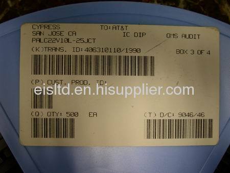
PART NUMBER | CY7C1423JV18-267BZXC |
BRAND | Cypress Semiconductor [Cypress] |
PACKAGING | FBGA |
DATE CODE | 12+ |
PRICE | 2~2.8USD |
Summary | 36 Mbit density, Synchronous internally self-timed writes, FBGA, DDR-II SIO SRAM |
Description as follow:
The CY7C1423JV18-267BZXC is a 1.8V Synchronous Pipelined SRAM. It is equipped with Double Data Rate Separate I/O (DDR-II SIO) architecture. The CY7C1423JV18-267BZXC consists of two separate ports: the read port and the write port to access the memory array. The CY7C1423JV18-267BZXC has separate data inputs and data outputs to completely eliminate the need to "turn-around" the data bus required with common I/O devices. Access to each port is accomplished through a common address bus. Addresses for read and write are latched on alternate rising edges of the input (K) clock.
Parametrics
CY7C1423JV18-267BZXC absolute maximum ratings: (1)Storage Temperature:–65℃ to +150℃; (2)Ambient Temperature with Power Applied:–55℃ to +125℃; (3)Supply Voltage on VDD Relative to GND:–0.5V to +2.9V; (4)Supply Voltage on VDDQ Relative to GND:–0.5V to +VDD; (5)DC Applied to Outputs in High-Z:–0.5V to VDDQ + 0.3V; (6)DC Input Voltage:–0.5V to VDD + 0.3V; (7)Current into Outputs (LOW):20 mA; (8)Static Discharge Voltage (MIL-STD-883, M. 3015): > 2001V; (9)Latch-up Current:> 200 mA.
Features
CY7C1423JV18-267BZXC features: (1)36 Mbit density (4M x 8, 4M x 9, 2M x 18, 1M x 36); (2)300 MHz clock for high bandwidth; (3)2-word burst for reducing address bus frequency ; (4)Double Data Rate (DDR) interfaces (data transferred at 600 MHz) at 300 MHz ; (5)Two input clocks (K and K) for precise DDR timing: SRAM uses rising edges only; (6)Two input clocks for output data (C and C) to minimize clock skew and flight time mismatches; (7)Echo clocks (CQ and CQ) simplify data capture in high speed systems; (8)Synchronous internally self-timed writes; (9)1.8V core power supply with HSTL inputs and outputs; (10)Variable drive HSTL output buffers; (11)Expanded HSTL output voltage (1.4V–VDD); (12)Available in 165-Ball FBGA package (15 x 17 x 1.4 mm); (13)Offered in both Pb-free and non Pb-free packages; (14)JTAG 1149.1 compatible test access port; (15)Delay Lock Loop (DLL) for accurate data placement.
Diagrams

Related Search
Find more related products in following catalogs on Hisupplier.com
Company Info
Excellent Integrated System LIMITED [Hong Kong]
Business Type:Distributor/Wholesaler
Country/Region: Hong Kong
You May Like:
.gif)


Product (300)
- Integrated Circuit (233)
- ICs (66)
- Others (1)
